

Product Performance
World first laser nanofabrication system with in-situ 3D refractive index imaging functionality
To address these challenges, Innofocus developed the world-first intelligent laser nanofabrication system with our unique in-situ 3D refractive index imaging functionality i.e. HoloView 3DRI. The nanoFACTORY i-QPC model can achieve in-situ refractive index characterisation to help users obtain quantitative data which indicates the variation of refractive index with the parameters changing.
The nanoFACTORY i-QPC model allows on-line inspection of the fabrication outcomes and on-site correction of fabrication conditions, which totally revolutionises the laser nanofabrication sector. It greatly reduces the time span required for the fabrication and characterisation of photonic devices and chips like i-QPCs, meanwhile significantly increasing the laser fabrication accuracy and reproducibility. Users can apply these data to design and simulate the 3D optical waveguide structure to be fabricated, to achieve globally optimal result.
It represents the state-of-the-art and it is the world’s only commercially available high-resolution in-situ 3D refractive index distribution characterisation equipment. Users can now perform characterisation and optimise the fabrication results during the fabrication of sample, which greatly reduces the time cost involved. It enables users to obtain the optimum results in one shot. It provides unprecedented convenience for 3D optical waveguide and photonic chip processing. It provides more support for the industrial applications of laser nanofabrication such as optical communication, all-optical network and quantum optics. The equipment is expected to provide promising solution for the existing industry challenge faced by the development of i-QPCs.
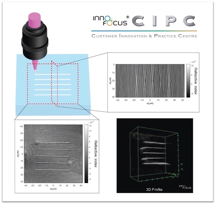
In-situ inspection of the refractive index difference
Quantitative measurement of both the surface and internal refractive index distributions of the components
Determine whether the material has been recharaterised by measuring the changes in its refractive index.
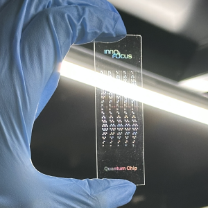
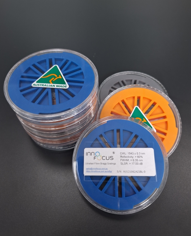
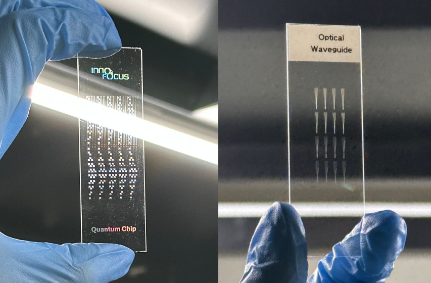
Industry applications