No products in the cart.

Microlens Array

One important branch of computational imaging is light field imaging. The core optical element in optical field imaging is the microlens array, which is made of transparent glass with many tiny lenses engraved on its surface to form an array structure for imaging. The relatively established process for making quartz microlenses is photoresist patterning with engraving, but there are various problems with this method.

Industry Challenge

+ ×

Low flexibility, high costs and long lead times

The commonly used photoresist method of producing graphics with engraving is not freely adjustable as the design of the lens needs to be determined by the mask plate graphics, and is costly, requiring processing of the mask plate for each new design of the lens array. In addition, each new design involves the fabrication of a new mask plate, resulting in a complicated and time-consuming process.

+ ×

Surface morphology cannot be precisely controlled, impossible to make aspheric lenses and high numerical aperture microlenses

As photolithography is a process for producing two-dimensional graphics, there is no direct control over the three-dimensional surface morphology of the lens fabricated. However, the focal length and image quality depend heavily on the surface morphology. Therefore, the focal length of the lens and the quality of image are seriously compromised when the surface morphology cannot be accurately controlled. In addition, due to the method of forming an arch by heating, the most likely surface morphology to be formed by thermal stabilisation is spherical according to the principle of uniform distribution of heat deformation, which cannot be accurately controlled. Furthermore, the resolution of imaging is greatly limited because the method of heating the surface to form an arch does not allow for the creation of lenses with a small radius of curvature to achieve high numerical apertures.

+ ×

Low uniformity

As controlled by heating, the curvature of each lens depends on the temperature applied to that lens. The difference in temperature will cause a difference in curvature and thus affecting the focal length. Also, even if the temperatures are all the same, there is no guarantee that each lens will develop the same change in curvature under heated conditions. Therefore the uniformity of the lens array is not guaranteed.

+ ×

Limited choices of photoresists

This process has three requirements for photoresists: 1) photosensitivity to UV light. 2) can be deformed by heat to form an arch. 3) The ability to resist argon-ion engraving for pattern transfer. Only particular photoresists can meet these requirements at the same time and so the choice is severely limited.

+ ×

Low yield rates

Even though the exposure process can be consistently controlled, without accurate control of its surface morphology during the heating process, the quality of each array of microlens is difficult to maintain. This results in low yield and repeatability.

Product Performance

Low cost and short time consuming

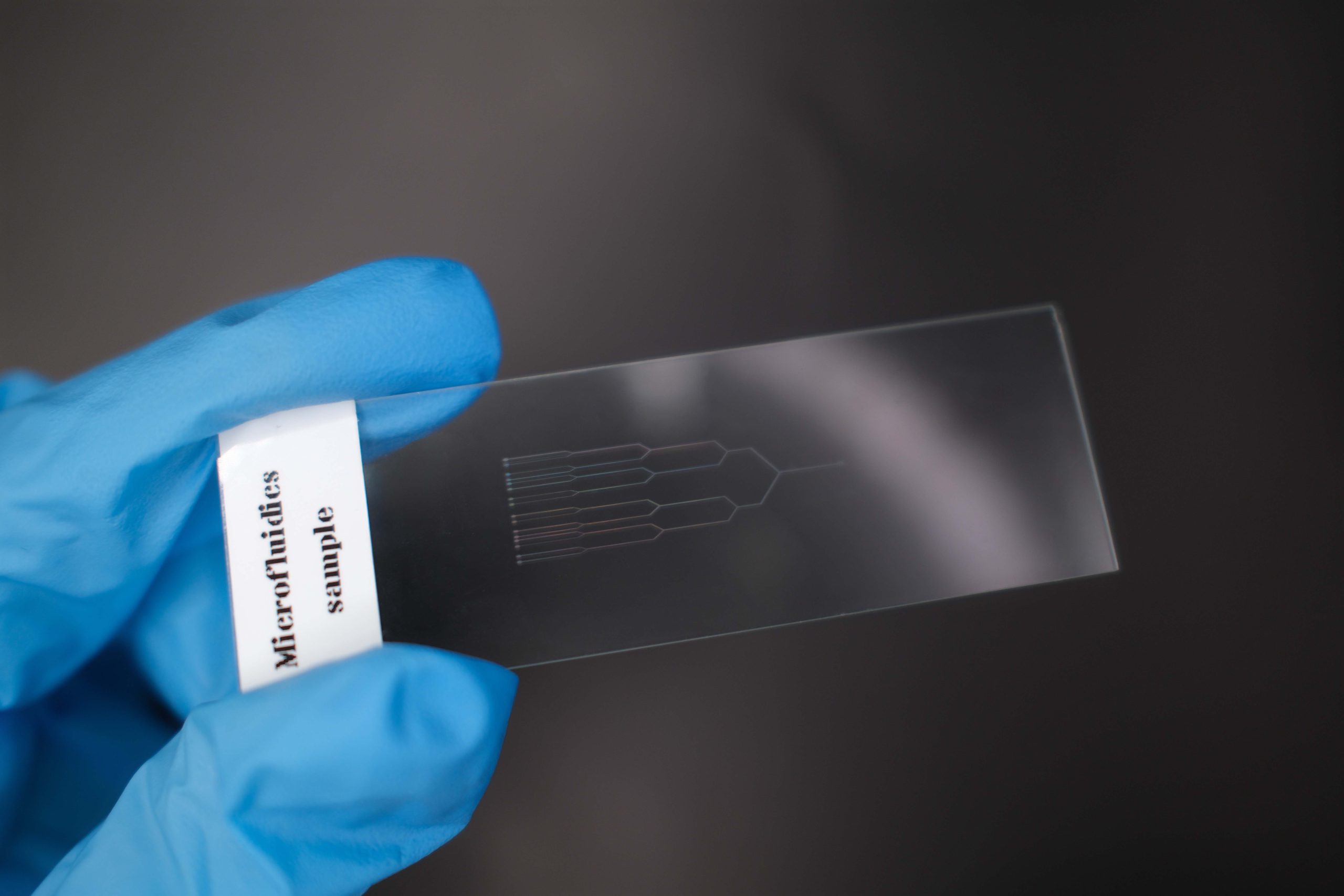
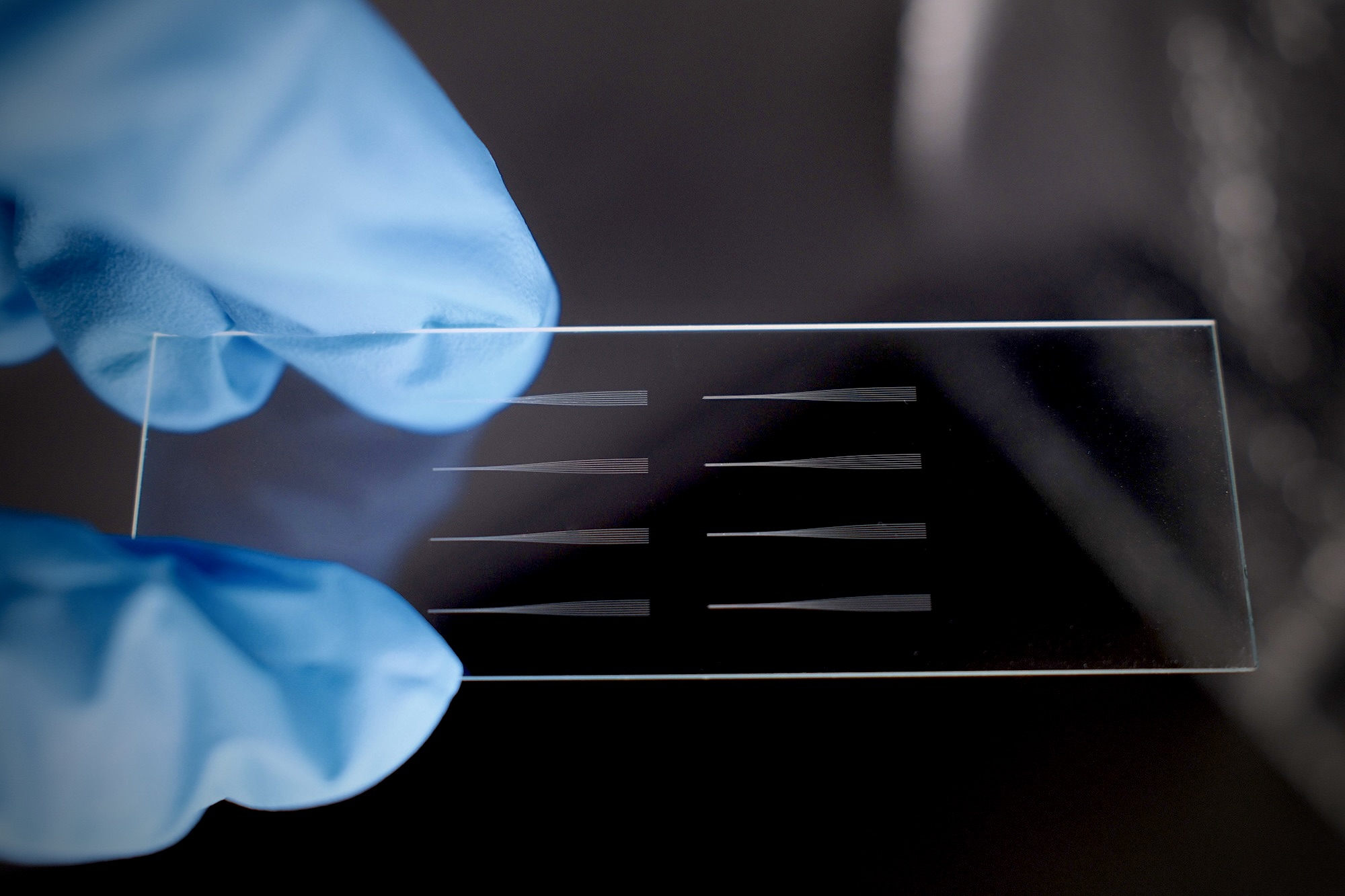
The cost of laser processing is extremely low as no mask production is required, and each new lens array design only requires the generation of a new processing file, allowing for rapid design optimisation comparisons


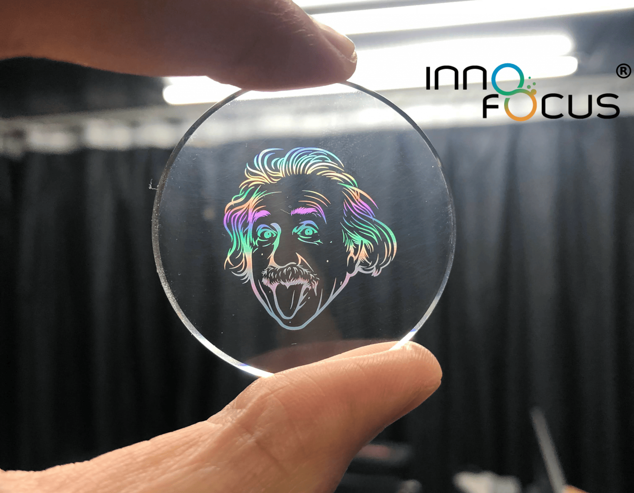
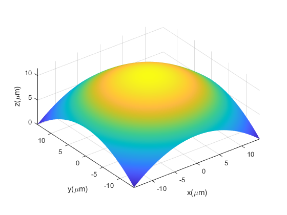
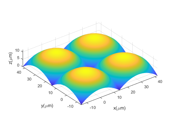
Precise 3D surface control

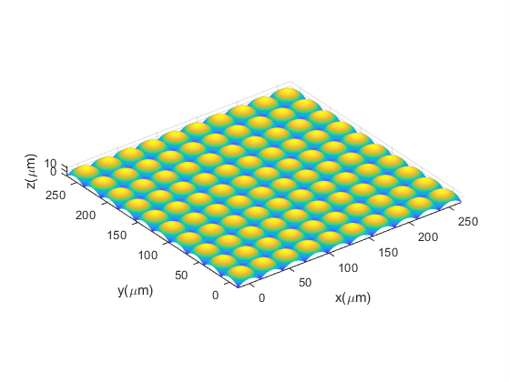
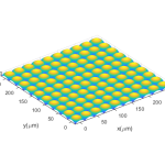
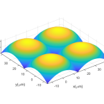
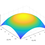
The spatial position of each microlens is used to create the surface profile of the microlens accordingly, resulting in a microlens array that meets the specific light field distribution.


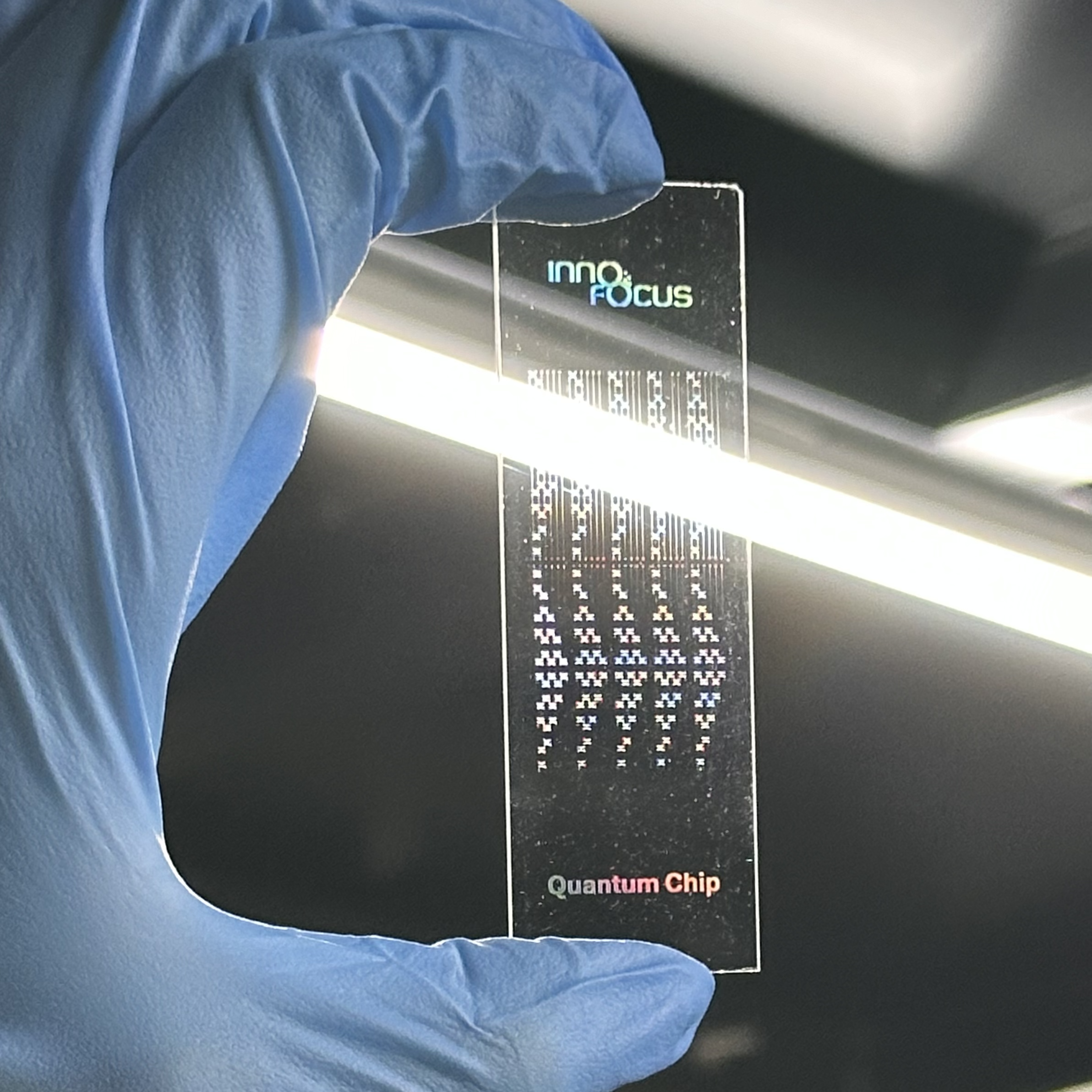
Fabrication of high quality achromatic aspherical microlens array structures

Thanks to the precise control of the structure’s three-dimensional surface morphology by laser nano-3D printing technology, the accurate processing of microlenses of arbitrary design can be achieved. The errors in the surface profile can be controlled within 10nm to sufficiently satisfy the fabrication demands.


High yield rates

Accurate control of the quality of microlens arrays can be achieved on the basis of high accuracy and uniformity, resulting in high yield rates.


1. Polymer mask etching

1. Polymer mask etching

This mainly includes two steps: 1) Fabrication of microlens array structures in polymers using laser nano 3D printing 2) The polymeric microlens array is then used as a mask to transfer the pattern onto the quartz substrate by means of etching
More
2. Laser direct writing in quartz glass coupled with selective acid etching

2. Laser direct writing in quartz glass coupled with selective acid etching

This mainly includes two steps: 1) A high power laser is used to introduce a phase transition directly inside the quartz glass by means of a femtosecond laser to write the anti-structure of the microlens array 2) Using selective acid etching to remove the area that need to be etched.
More
×

Applications

Widely used in virtual reality, automotive lighting, optical imaging, radar ranging, infrared imaging
More
×
Contact Us

Contact Information

Innofocus Photonics Technology Pty Ltd

Unit 10/17 Helen Street, Heidelberg West 3081, Victoria, Australia

+61 3 9077 8119

"*" indicates required fields